High-throughput Fabrication on Thin-film Materials
High-throughput Fabrication on Thin-film Materials


Yong Jiang Professor at the University of Science and Technology Beijing, China; Winner of the National Science Fund for Distinguished Young Scholars; Changjiang (Yangtze River) Scholar
Shouguo Wang Professor at the University of Science and Technology Beijing, China; Winner of the National Science Fund for Distinguished Young Scholars
Yang Sun Researcher at the Institute of Physics Chinese Academy of Sciences; Winner of the National Science Fund for Distinguished Young Scholars
Xiaolu Pang Professor at the University of Science and Technology Beijing, China
【Chief Members】
Yong Jiang Professor at the University of Science and Technology Beijing
Shouguo Wang Professor at the University of Science and Technology Beijing
Yang Sun Researcher at the Institute of Physics Chinese Academy of Sciences
Xiaolu Pang Professor at the University of Science and Technology Beijing
【Research Background】
Magnetic thin film, multiferroic thin film, high-κ dielectric thin film, transparent conducting film, and hard thin film are some of the commonly used thin films. These materials play an increasingly important role in the manufacture of large-scale integrated circuits, information storage and processing units, electronic components, fuel cells, and in the enhancement of wear and corrosion resistances of materials. In recent years, with increasing investment and favorable policies of the state in the fields of high-tech and advanced manufacturing, China has made significant progress in the areas of novel material design, micro- and nano-manufacturing technology, chip design, etc., which also provide an unprecedented opportunity for the development of thin film materials. It is well-established that when thin film preparation methods, such as magnetron sputtering, pulsed laser deposition, molecular beam epitaxy, and chemical vapor deposition, are combined with micromachining processes, such as photolithography and ion beam etching, the film should be one of the materials that can achieve high-throughput preparation easily. The development of high-throughput fabrication techniques for thin film materials provides a theoretical and experimental basis for accelerating the discovery of the characteristics of composition, development, structure, and performance of bulk materials.
【Research Objectives】
Initial array and gradient distribution of composition has already been achieved in high-throughput preparation of thin film materials, but simultaneously achieving array or gradient distribution of composition and microstructures has not yet been realized. The challenges encountered include those of technical, such as the precise control of physical fields, which include temperature, magnetic field, and electric field, which has proven to be difficult in the process film material preparation, and key scientific questions concerning material diffusion, phase change, crystal nucleation and growth, etc. Our team intends to conduct research on relevant topics for achieving high-throughput preparation and rapid screening of thin film materials.
【Main research areas】
1. Research on technology for controlling physical fields including temperature, magnetic, electric and plasma;
2. Research on key technologies for diffusion/crystallization in high-throughput preparation of thin film materials;
3. High-throughput preparation techniques through other means for large-area uniform film materials;
4. Establishment of effective technical techniques for high-throughput preparation of low-dimensional materials.
【Significant Research Progress】
1. Research on functional SmNiO3 thin film
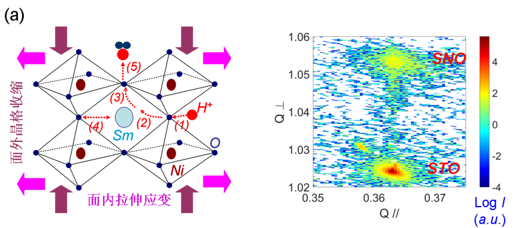
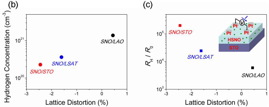
For the first time, the hydrogen and oxygen elements of rare-earth perovskite nickelates such as SmNiO3 before and after hydrogen-induced phase transition were quantitatively characterized. It was found that during hydrogen-induced phase transition, although the rate of change of electrical resistance of SmNiO3 thin film materials under biaxial tensile stress is higher than that under partial compressive stress, the actual content of hydrogen is insignificant. The experimental results invalidate the explanation for primary mechanism underlying hydrogen-induced phase transition of rare-earth perovskite nickelates, and prove that the insulating phase of rare-earth perovskite nickelates, which produce strong electronic localized state is not directly related to the doping amount of hydrogen, but rather to the fact that the migration of hydrogen in the material creates a localized defect in the metastable state. This is of great scientific significance for understanding the mechanism underlying phase transition of hydrogen-induced metal insulators of perovskites, which belong to the strongly correlated d-electron system, and for further utilizing the phase transition to design and prepare strongly correlated electron devices. The research results were published in Nature Communications 10, 694(2019).


Fig.1 RSM graph of SmNiO3 thin film under biaxial tensile stress on STO single crystal substrate (a); Hydrogen content after hydrogen-induced phase transition of SmNiO3 thin films with different lattice strains on STO, LAO, LSAT, and single crystal substrates (b); and the rate of change of electrical resistance (c).
2. Research on two-dimensional molybdenum trioxide
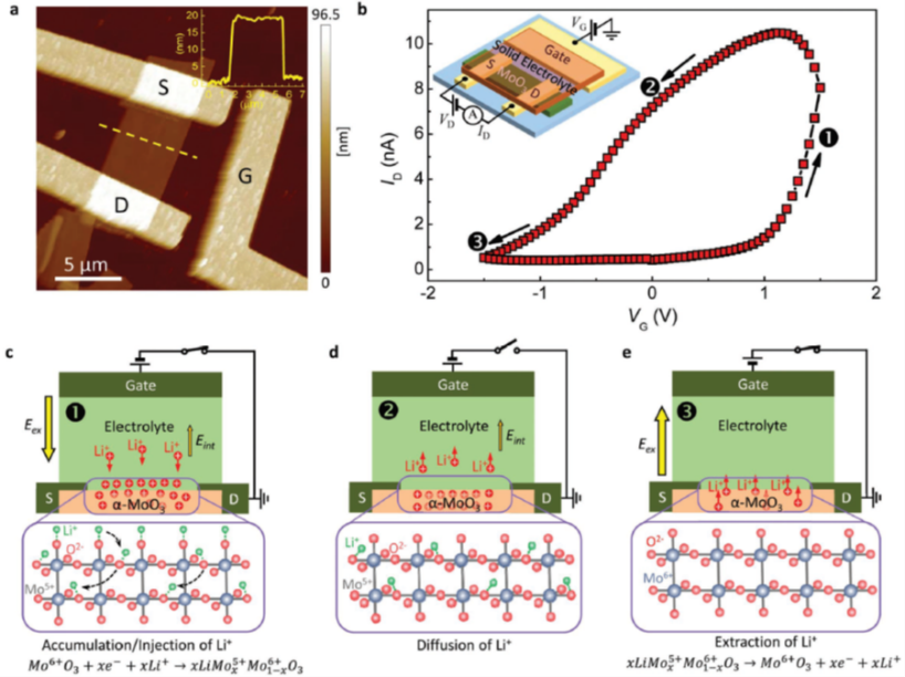
An all-solid-state synaptic transistor was fabricated using a Li-ion solid electrolyte as the isolation gate. Under the action of the gate voltage, the polymorphic reversible change of α-MoO3 channel resistance under low conductance conditions was realized with the injection and extraction of Li ions in the two-dimensional α-MoO3 material, and behaviors, such as changes in the synaptic weights, were successfully simulated. This device can also realize change in channel conductance under vacuum conditions, thereby eliminating the dependence on the external environment. The device is also expected to realize the preparation of large-scale device arrays. The three-layered neural network (784×300×10) built by Li-ion synaptic transistor arrays was combined with a backpropagation algorithm for training and recognition of handwritten digital library with a recognition accuracy of 87.3%. This work demonstrates the feasibility of using Li-ion solid-state electrolytes to achieve low-power all-solid-state synaptic transistors and provides a novel way of achieving large-scale synaptic transistor array preparation to develop high-efficiency neuromorphic computing networks. The research results were published in Advanced Functional Materials 28, 1804170 (2018).

Fig.2 Structure, electron transport properties, and Lithium ion injection/extraction mechanism of synaptic transistors based on α-MoO3
